DCPU - From Logic Gates to a Functioning Processor
Sep 30, 2023 | Github: github.com/dma-neves/dcpu
Index
- 1. Introduction
- 2. Background
- 3. Buliding an ALU
- 4. State, Memory and Clock
- 5. Instruction Set Architecture
- 6. Control Unit
- 7. Executing a Program
- 8. Assembler
- 9. FPGA
1. Introduction
Since a long time, I've found computers fascinating machines and wondered how they worked. My first attempts at understanding these complicated systems arose during middle school while playing around with redstone circuitry in Minecraft. I wondered how one could go from basic digital circuits to executing complex programs as we are used to. But it's fair to say that the jump from some simulated wiring in a video game to a functional computer was a bit ambitious. Fast forward to 2020, during my second year of University, and after learning about Digital Systems, Computer Architectures and Operating Systems, I felt I finally had the necessary base knowledge to make the leap. With some basic knowledge of VHDL I decided to design and implement a simple ALU, and then went on from there.
In this guide, I will try to guide you through the steps I went through (excluding all the original trial and error) to build a primitive CPU in VHDL using logic gates as the foundational building blocks. Even though VHDL allows one to design and implement complex systems using high-level behavioral descriptions (that are then compiled down to logic gates), I tried to purposely avoid these high-level features (like processes) in order to achieve a deeper and more complete understanding of the inner workings of a CPU.
It's important to note that the CPU we will be building is in no way revolutionary, impressive or particularly well designed. Hence the the name DCPU (Dumb CPU). Rather, the CPU is supposed to be as simple as possible, while still including most of the important functionalities a CPU needs to be usable.
Note: The source code of this project can be found in my Github repository. Also note that the original project is a 16 bit CPU, while the code I provide in this document follows mostly an 8 bit design for compactness.
2. Background
Before diving into the implementation, we first need to establish some basic background information and concepts like the Von Nuemann Architecture, transistors, logic gates, Hardware Description Languages and FPGAs. If you are already familiar with these concepts, skip to the next chapter.
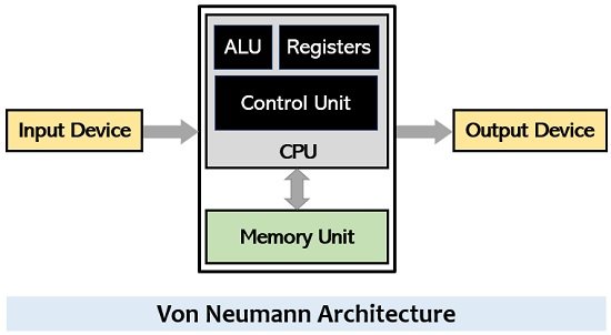
In 1945, John Von Neumann proposed an architecture for an electronic digital computer (Fig.2). This would end up becoming the basis for pretty much all computer architectures, even to this day. The architecture proposes a system with the following essential components:
- A processing unit with an ALU (Arithmetic Logic Unit) and registers. A register stores a value in a set of bits.
- A control unit including an instruction register and a program counter.
- A memory unit that stores data and instructions.
- Input and output mechanisms.
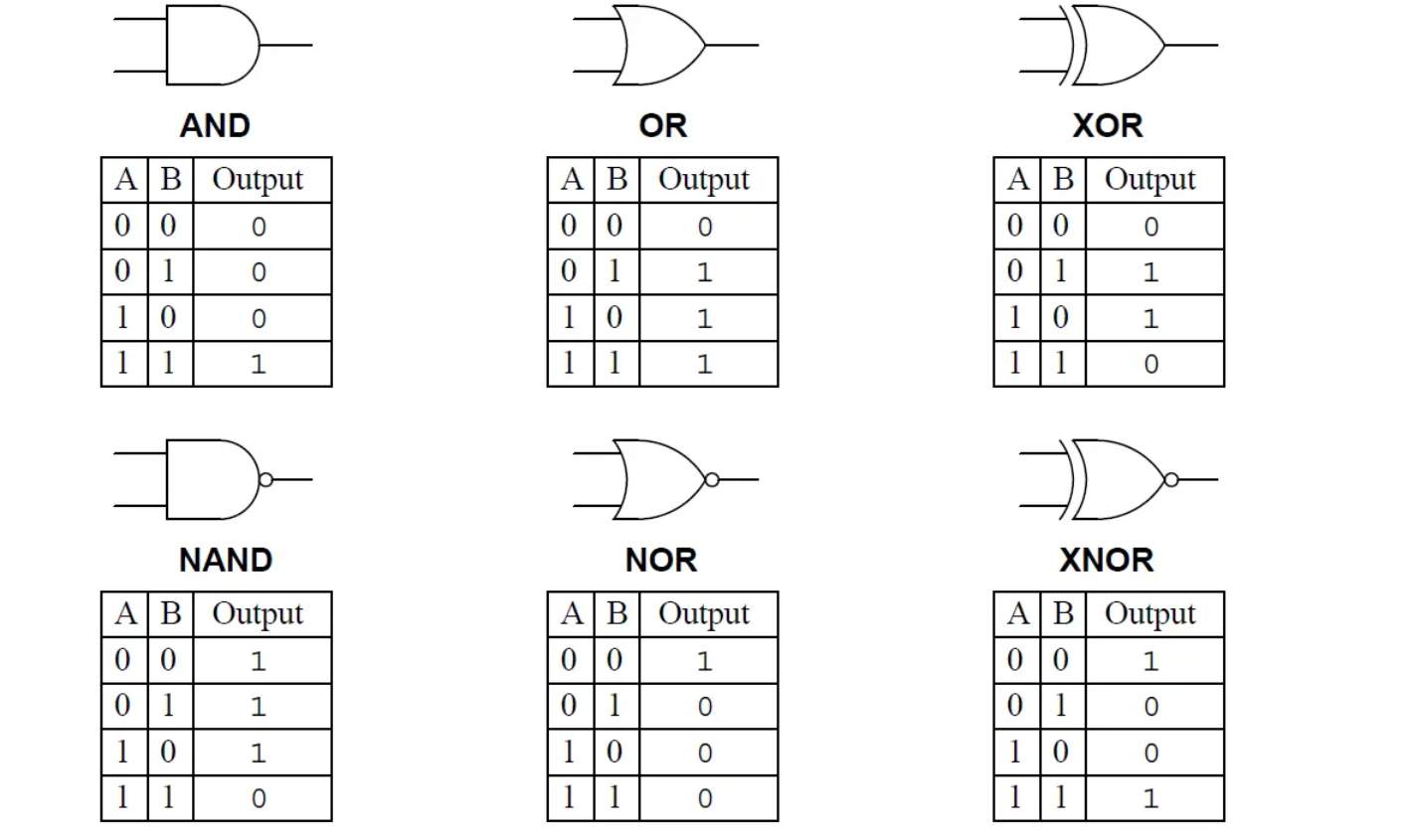
Fundamentally, computers are made of billions of transistors. These transistors are combined to form logic gates. With logic gates we can build any digital system, including our CPU. A logic gate takes one or two bits as input and outputs a single bit. Fig.3 shows all the basic logic gates. AND outputs 1 if both inputs are 1 otherwise 0, OR outputs 1 if any of the inputs is 1 and XOR outputs 1 if exactly one of the inputs is 1. The bottom three logic gates are the same as the first three but followed by a NOT logic gate. A NOT logic gates that takes a single input and outputs its negation. A circle succeeding a logic gate's symbol, indicates a negation. We can combine these logic gates to add two numbers represented in binary form, perform more complex arithmetic operations, store data and even implement a modern Intel or AMD CPU if we were clever enough.
In order to develop our own CPU, we need to somehow create or represent a circuit composed of these logic gates. One way would be to buy some chips with logic gates and assemble them on a breadboard. Another option would be to design an manufacture an actual microchip. Given that both these options don't scale very well, can cost some money and aren't very debug friendly, a more convenient and cheaper alternative is to design our circuits using a hardware description language like VHDL. These languages allow one to describe a digital system using code. With the VHDL code we can then simulate the circuit on our computer, or "upload" it to an FPGA (Field Programmable Gate Array). An FPGA is an integrated circuit that can be configured to behave as "any" circuit we want.
Note that this guide will not include an in depth tutorial on VHDL, so even though the VHDL we'll be writing is very basic, you might want to watch some basic VHDL tutorial first. I will also assume that you have some basic knowledge of programming and concepts like stacks, pointers, binary representation, bit manipulation, etc. In terms of tools, I personally used ghdl and GTKWave to simulate VHDL and visualize the simulation on my computer, and used the Intel Quartus II software to program my ALTERA FPGA CycloneII EP2C5T144.
3. Building an ALU
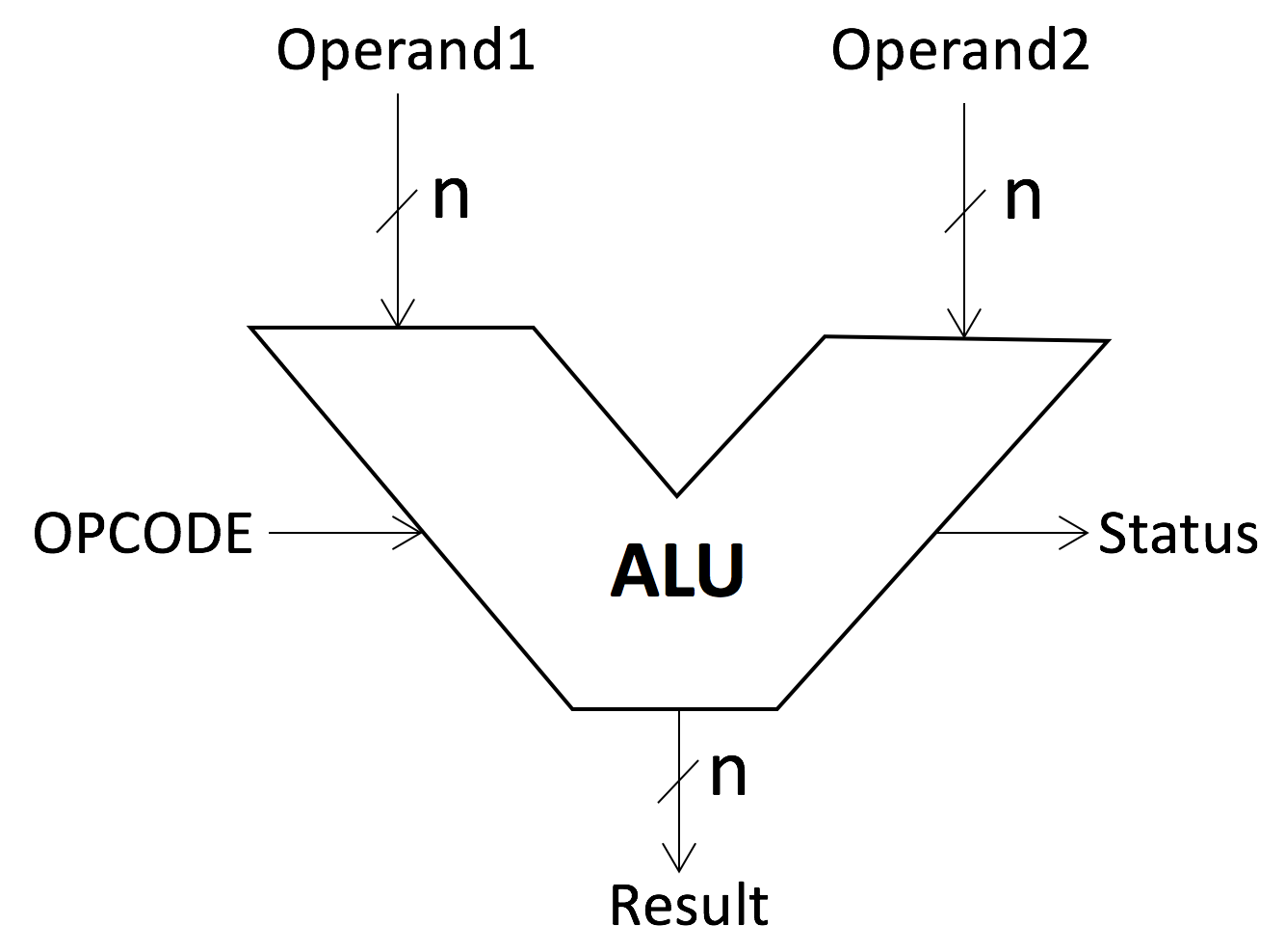
Our first step is to build an ALU (Arithmetic Logic Unit). This unit is responsible for carrying out all the math operations a CPU might need to perform. A simple ALU (Fig.4), takes as inputs two binary numbers (operands) and an operation code (opcode), and outputs a binary number (result) and some flags (status) that correspond to the result of performing the specified operation on the operands.


The first operation we'll implement is addition. If we want to add two bits A and B, we can use the circuit seen in Fig.5, a half-adder. The AND gate
computes the carry bit and the XOR gate the result bit. If A and B are 1 then the result is 0 and the carry is 1. If A and B are 0 then the result is 0 and the carry is 0.
If only A or only B is 1, the result is 1 and the carry 0. To make a full-adder (Fig.6) that takes as input two bits A and B, and a carry bit Cin, we simply chain two
half-adders and OR the carry bits. We can implement this circuit in VHDL as follows:
    entity FullAdder is

    Port(
        carryIn : IN STD_LOGIC;
        a : IN STD_LOGIC;
        b : IN STD_LOGIC;

        result : OUT STD_LOGIC;
        carryOut : OUT STD_LOGIC
    );

    end FullAdder;

    architecture Behavioral of FullAdder is

    signal result_0, carry_0, carry_1 : STD_LOGIC;

    begin
    result_0 <= a xor b;
    carry_0 <= a and b;
    carry_1 <= result_0 and carryIn;
    result <= result_0 xor carryIn;
    carryOut <= carry_0 or carry_1;
    end Behavioral;
To make an adder that adds two numbers A and B of N bits, we can use N full-adders. We add the first bits from A and B using
the first full-adder, passing 0 as the carry in, then add the second bits from A and B using the second full-adder, routing the carry out from the first full-adder to
the carry in from the second full-adder, and so on. The following code implements an 8 bit adder:
    entity Adder is
    Port(
        a : IN STD_LOGIC_VECTOR(7 downto 0);
        b : IN STD_LOGIC_VECTOR(7 downto 0);

        result : OUT STD_LOGIC_VECTOR(7 downto 0);
        carryOut : OUT STD_LOGIC
    );
    end Adder;

    architecture Behavioral of Adder is
    -- Components code here
    signal co_0, co_1, co_2, co_3, co_4, co_5, co_6, co_7 : STD_LOGIC;

    begin
    S0 : FullAdder port map ('0', a(0), b(0), result(0), co_0);
    S1 : FullAdder port map (co_0, a(1), b(1), result(1), co_1);
    S2 : FullAdder port map (co_1, a(2), b(2), result(2), co_2);
    S3 : FullAdder port map (co_2, a(3), b(3), result(3), co_3);
    S4 : FullAdder port map (co_3, a(4), b(4), result(4), co_4);
    S5 : FullAdder port map (co_4, a(5), b(5), result(5), co_5);
    S6 : FullAdder port map (co_5, a(6), b(6), result(6), co_6);
    S7 : FullAdder port map (co_6, a(7), b(7), result(7), co_7);
    carryOut <= co_7;
    end Behavioral;
Logic operations on N bit numbers are easily implemented by performing the operation (like AND, OR, NOT, etc) on all the N inputs.
Since they are logic operations, they are directly implemented by a single logic gate. For example an AND operation between two 8 bit numbers
can be implemented as follows:
    entity And_8 is
    Port(
        a : in STD_LOGIC_VECTOR(7 downto 0);
        b : in STD_LOGIC_VECTOR(7 downto 0);

        a_and_b : out STD_LOGIC_VECTOR(7 downto 0)
    );
    end And_8;

    architecture Behavioral of And_8 is

    begin
    a_and_b(0) <= a(0) and b(0);
    a_and_b(1) <= a(1) and b(1);
    a_and_b(2) <= a(2) and b(2);
    a_and_b(3) <= a(3) and b(3);
    a_and_b(4) <= a(4) and b(4);
    a_and_b(5) <= a(5) and b(5);
    a_and_b(6) <= a(6) and b(6);
    a_and_b(7) <= a(7) and b(7);
    end Behavioral;
The next challenge is dealing with subtractions and negative numbers. The most popular approach to this problem is using the two's compliment method. We assume that the the binary digit with the greatest place value (the left most) in a binary number represents the number's sign. 0 corresponds to a positive number and 1 corresponds to a negative number. Positive numbers are represented in the same way as before, while negative numbers are encoded differently. To represent a negative number in two's compliment, we use the following method:
- Starting with the equivalent positive number.
- Invert (or flip) all bits.
- Add 1 to the entire inverted number, ignoring any overflow
3 (0b00000011) to -4 (0b11111100), this is 3-4, gives us 0b11111111, which encodes the value -1.
By adding a module to our ALU that negates a value, we can then implement subtractions by performing negations followed by additions. This is, A-B
can be implemented as A+(-B). A negation module can be implement as follows using the previous adder and an 8 bit NOT operator:
    entity Negate is
    Port(
        a : in STD_LOGIC_VECTOR(7 downto 0);
        neg_a : out STD_LOGIC_VECTOR(7 downto 0);
        overflow : out STD_LOGIC
    );
    end Negate;

    architecture Behavioral of Negate is

    -- Components code here
    signal not_a : STD_LOGIC_VECTOR(7 downto 0);

    begin
    N: Not_8 port map(a, not_a);
    S: Adder port map(not_a, "00000001", neg_a, overflow);
    end Behavioral;

The final piece we need to build the ALU is a multiplexer, which given a set of input values, allows us to select a specific one.
Assuming a multiplexer receives a set of inputs I0, I1, ..., IN
(each input can be a single bit or a binary value) and a selector S, it outputs the value In, where n is the index selected by S. This is,
if S is 0b0 the output is I0, if S is 0b1 the output is I1, if S is 0b10 the output is I2 and so on. Such a component can be easily implemented
using AND gates connecting each input I with the necessary S value (NOT gates used for the bits that should be zero) and a final OR gate
combining all the intermediate outputs. Fig.7 shows a multiplexer circuit with 4 input values and a two bit selector S. This multiplexer can be implemented as follows:
    entity Mux4 is
    Port(
        I0, I1, I2, I3 : in STD_LOGIC_VECTOR(7 downto 0);
        sel : in STD_LOGIC_VECTOR(1 downto 0);
        o : out STD_LOGIC_VECTOR(7 downto 0)
    );
    end Mux4;

    architecture Behavioral of Mux4 is
    signal I0_s, I1_s, I2_s, I3_s : STD_LOGIC_VECTOR(7 downto 0);
    begin

    I0_s(0) <= I0(0) and (not sel(0)) and (not sel(1));
    //I0_s(...) <= ...
    I0_s(7) <= I0(7) and (not sel(0)) and (not sel(1));

    I1_s(0) <= I1(0) and (not sel(0)) and sel(1);
    //I1_s(...) <= ...
    I1_s(7) <= I1(7) and (not sel(0)) and sel(1);

    I2_s(0) <= I2(0) and sel(0)) and (not sel(1));
    //I2_s(...) <= ...
    I2_s(7) <= I2(7) and sel(0)) and (not sel(1));

    I3_s(0) <= I3(0) and sel(0)) and sel(1);
    //I3_s(...) <= ...
    I3_s(7) <= I3(7) and sel(0)) and sel(1);

    end Behavioral;
With an adder, logic operators, a negator and some multiplexers, we can finally build our ALU. Lets consider that the ALU will support 8 different
operations. Our opcode will therefore be specified by a 3 bit value (since 2^3 = 8). Tab.1 shows the 8 operations we will support.
| Opcode | Name | Description |
|---|---|---|
| 0b000 | add | A + B |
| 0b001 | sub | A - B |
| 0b010 | inc | A + 1 |
| 0b011 | dec | A - 1 |
| 0b100 | neg | -A |
| 0b101 | not | ~A |
| 0b110 | and | A ∧ B |
| 0b111 | or | A v B |
Fig.8 shows a diagram of the ALU that implements these 8 operations. It receives two 8 bit input operands A and B as well as an input opcode. For
output, we have a single 8 bit result and three flags: overflow, negative and zero.
The ALU contains the Adder, Negate, NOT, OR and AND components we
discussed earlier, a set of multiplexers and some auxiliary gates. The first operand of the Adder is always A, while the second is selected by a multiplexer
that can either select B (add), 1 (inc), -1 (dec) or the result of the Negate component (sub). The Negate input is selected by a multiplexer that can either
select A (neg) or B (sub). All the other components simply operate over A and B (operations: not, and, or). The final result is selected by a multiplexer
that can either select the Negate output (neg), the NOT output (not), the AND output (and), the OR output (or) or the Adder output (operations: add, inc, dec, sub).
The overflow flag can be set either by the Adder component or the Negate component, and the negative and zero flag simply check if the result is negative or
zero.
Notes: In this circuit there are actually two adders given that there is also an adder embedded in the Negate module. We could refine the design and share a single Adder for both purposes, but this solution is slightly more convenient and allows us to implement the subtraction operation easily. Note also that the negation performed on the selector of Mux5 is somewhat unnecessary. It is present in this schematic just to achieve a more convenient layout of the inputs.

This ALU can be implemented in VHDL as follows:
    entity ALU is

    Port (
        a : IN STD_LOGIC_VECTOR(7 downto 0);
        b : IN STD_LOGIC_VECTOR(7 downto 0);
        opc : IN STD_LOGIC_VECTOR(2 downto 0);

        result : OUT STD_LOGIC_VECTOR(7 downto 0);
        zeroF : OUT STD_LOGIC;
        negativeF : OUT STD_LOGIC;
        overflowF : OUT STD_LOGIC
    );
    end ALU;

    architecture Behavioral of ALU is

    signal isc, iac, inc, addC, negOF, overf, carry : STD_LOGIC;
    signal opc_2 : STD_LOGIC_VECTOR(1 downto 0);
    signal opc_M5 : STD_LOGIC_VECTOR(2 downto 0);
    signal om4, om2, om5, addR, negA, notA, andAB, orAB : STD_LOGIC_VECTOR(7 downto 0);

    -- Components code here

    begin
    isc <= (not opc(0)) and (not opc(1)) and opc(2)        -- Is Sub Code (001)
    iac <= (not opc(0)) and (not opc(1)) and (not opc(2))  -- Is Add Code (000)
    inc <= opc(0) and (not opc(1)) and (not opc(2))        -- Is Neg Code (100)


    opc_2(0) <= opc(0);
    opc_2(1) <= opc(1);

    MUX4_M: Mux4 port map (B, negA, "00000001", "11111111", opc_2, om4);
    MUX2_M: Mux2 port map (A, B, isc, om2);

    ADDER_M: Adder port map(A, om4, addR, addC);
    NEGATE_M: Negate port map(om2, negA, negOF);
    NOT_M: Not_8 port map(A, notA);
    AND_M: And_8 port map(a, b, andAB);
    OR_M: Or_8 port map(a, b, orAB);

    opc_M5(0) <= opc(0);
    opc_M5(1) <= opc(1);
    opc_M5(2) <= not opc(2);

    MUx5_M: Mux5 port map (negA, notA, andAB, orAB, addR, opc_M5, om5);

    IS_NEGATIVE_M: isNegative port map (om5, negativeF);
    IS_ZERO_M: isZero port map (om5, zeroF);

    carry <= addC and iac;
    overf <= negOF and inc;
    overflowF <= carry or overf;

    result <= om5;
    end Behavioral;
4. State, Memory and Clock

| S | R | Qn+1 |
|---|---|---|
| 0 | 0 | Qn |
| 0 | 1 | 0 |
| 1 | 0 | 1 |
| 1 | 1 | Indeterminate |
With the ALU built, we can now perform "all" the mathematical operations we need. However, we need some way to store the results of these operations and data in general.
Fortunately, some smart physicists in the early 20th century found a way to store information using circuits, called multi-vibrators, that can easily be reproduced
using transistor-based logic gates. Fig.9 shows the schematic of a SR Flip-Flop. A SR Flip-Flop stores a state Q (note: Q' = ~Q) and provides two inputs
to set the state (Q = 1) and reset the state (Q = 0). Considering that the Flip-Flop is in the current state Qn, Tab.2 presents its truth table. Given that the
NOR gate's output is only 1 when both outputs are 0, we can see that if Q is 1 and Q' is 0, setting S to 1 results in Q changing to 0 and therefore Q' to 1. While
setting R to 0 results in Q' changing to 1 and therefore Q to 0. If this doesn't seem clear, Ben Eater has a great comprehensive video
on this circuit alone.
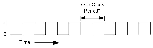
Given that computer programs must perform a sequence of instructions, and not just a single operation, CPUs need some sort of sequencing mechanism. This is where the clock comes in. Inside every computer is a clock generator, usually a crystal oscillator, that generates a pulse (or voltage) at even intervals as seen in Fig.10. The CPU can then use this clock to perform an instruction step on each clock cycle (More information on this in chapter 6). This means that state changes inside a CPU must also occur synchronously with the clock. Ideally, the state of a Flip-Flop inside a CPU, should only be updated during a clock pulse (a change of signal from 0 to 1, or from 1 to 0) to eliminate any glitches related to signal propagation delays and to ensure state changes happen in sync with the rest of the CPU.

| D | En | Qn+1 |
|---|---|---|
| 0 | 1 | 0 |
| 1 | 1 | 1 |
| X | 0 | Qn |
Fig.11 shows the schematic for a D Flip-Flop. This Flip-Flop is similar to the previous one, but receives an enable signal as input, which can be connected to the clock signal (or connected to an AND gate with the clock signal) to ensure that any state changes issued to the Flip-Flop are only triggered during a clock pulse*. It also combines the previous S and R inputs into a single Data input. Tab.3 presents the D Enable Flip-Flop's truth table.
Note the asteriscs I added when mentioning the clock pulse in the previous paragraph. This circuit does not in fact trigger the update during a clock pulse, but rather, allows updates whenever the clock is set to 1. We can refine the Flip-Flop to only trigger during a clock pulse by utilizing a master-slave Flip-Flop system. We won't get into details on how a master-slave Flip-Flop works, but it basically involves chaining two Flip-Flops and using the first's input as the second's enable input. Ben Eater has a great video going through a master-slave JK Flip-Flop if you're interested (and also a video on JK Flip-Flops). Given that implementing one of these Flip-Flops manually (using logic) in VHDL can be prone to latching bugs, we will make an exception, and implement the D Flip-Flop using a VHDL process. This Flip-Flop includes a reset input which just sets the input to zero, and an enable input which sets Q to the input data D whenever there is a pulse from 0 to 1:
    entity DFlipFlop is

    Port(
        D, En, R : in STD_LOGIC;
        Q : OUT STD_LOGIC
    );

    end DFlipFlop;

    architecture Behavioral of DFlipFlop is

    begin

        process (D, En, R) begin
            if(R = '1') then
            Q <= '0';
            elsif (En'event and En = '1') then
            Q <= D;
            end if;
        end process;

    end Behavioral;
With a D Flip-Flop, implementing an 8-bit register is trivial. We simply use a D Flip-Flop per bit to store the 8-bit value. We can implement an 8-bit register in VHDL as follows:
    entity Register_8b is
    Port(
        En, R : in STD_LOGIC;
        DIn : in STD_LOGIC_VECTOR(7 downto 0);
        DOut : out STD_LOGIC_VECTOR(7 downto 0)
    );
    end Register_8b;

    architecture Behavioral of Register_8b is
    -- Components code here
    begin
        DFF_0: DFlipFlop port map (DIn(0), En, R, DOut(0));
        DFF_1: DFlipFlop port map (DIn(1), En, R, DOut(1));
        DFF_2: DFlipFlop port map (DIn(2), En, R, DOut(2));
        DFF_3: DFlipFlop port map (DIn(3), En, R, DOut(3));
        DFF_4: DFlipFlop port map (DIn(4), En, R, DOut(4));
        DFF_5: DFlipFlop port map (DIn(5), En, R, DOut(5));
        DFF_6: DFlipFlop port map (DIn(6), En, R, DOut(6));
        DFF_7: DFlipFlop port map (DIn(7), En, R, DOut(7));
    end Behavioral;
A memory module can be implemented as a large array of registers. In a memory module, each register must be accessible by an address.
The first register can be set to address 0b00000000, the second register to address 0b00000001 and so on. This addressing system can be
achieved by connecting the registers to a large demultiplexer. A demultiplexer implements the inverse operation of a multiplexer. With a
selector (the address), the demultiplexer routs an input value to one of the N outputs (N registers for example). Note that there are more efficient ways
(using less logic gates) of implementing a memory module. Since the focus of this project is the implementation of a CPU, and not necessarily memory
modules, I implemented the
RAM and
ROM
modules using VHDL processes.
5. Instruction Set Architecture
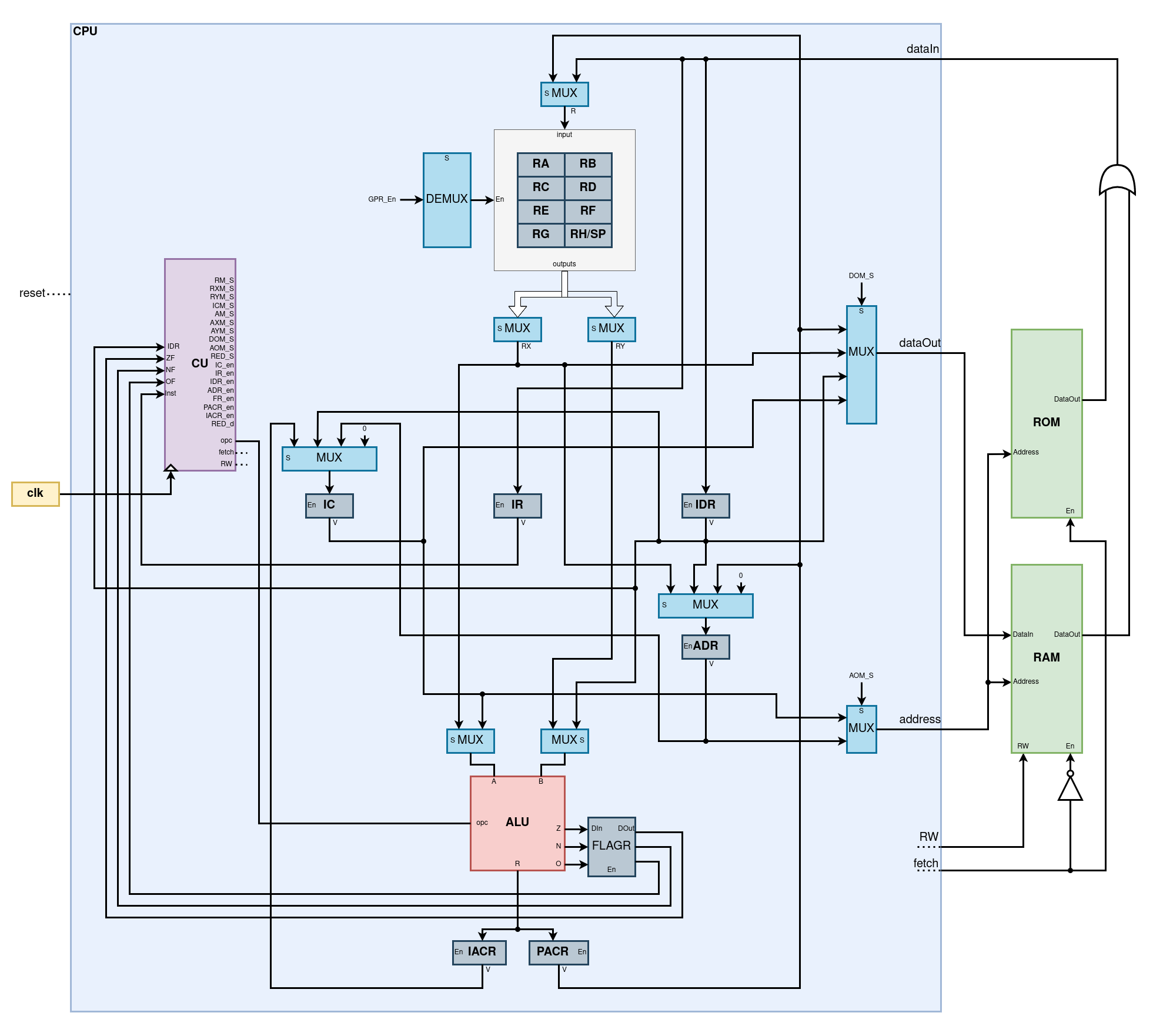
Now that we are able to perform operations and store and manipulate state, its time to define our CPU's architecture as well as its ISA (Instruction Set Architecture). A CPU's ISA, is simply the set of instructions it supports. As we discussed in chapter 1, following the Von Neumann architecture, our system should include an ALU, a memory module, a set of registers and a control unit. Fig.12 shows the schematic of the system we aim to build. It contains a control unit, two memory modules (a ROM to store a program and a RAM to store data), the ALU we implemented previously, a set of registers, and a set of multiplexers and demultiplexers (inverse multiplexer). In terms of registers, the CPU will have 8 general purpose registers (RA, RB, ..., RH), used to store temporary values during a program's execution, and 7 specialized registers:
- IC: Instruction Counter saves the address of the current instruction being executed.
- IR: Instruction Restister saves the instruction (the opcode) being executed.
- IDR:Instruction Data Register saves the data associated to the instruction being executed (more on this on chapter 6).
- ADR:Address Register saves an address that can be used to address the memory modules or to jump to the specified address/instruction.
- IACR:Instruction Accumulator Register saves the result of the ALU from an operation triggered by the instruction being executed.
- PACR:Program Accumulator Register saves the result of the ALU during a program counter increment (more on this on chapter 6).
- FLAGR:Flag Register saves the values of the flag values from the ALU.
With this architecture in mind, we can now define an ISA. For our CPU to be usable it needs to be at the very least Turing complete. Turing completeness refers to a system's ability to perform any computation that a Turing machine, allowing it to perform virtually any computation. In practice this requires our ISA to support conditional branches, some iteration mechanism and memory manipulation. We can achieve this by combining our ALU operations with some load and move operations to move data between registers and memory, a jump operation (jump to a specific instruction or address) and some conditional jump operations.
Additionally, as programs get more complex, having a stack becomes pretty essential, and for this reason, we will also include some basic support for a stack. Register RH will be used as the stack pointer, and we'll include an operation to subtract a value directly from it (useful when addressing variables stored in the stack). A stack also allows us to support functions as we can push both parameters and return addresses to the stack. The ADR register allows us to move said return addresses to it, and then perform the corresponding jump to the return address.
Finally, some instructions require some data to be specified alongside the instruction. For example to subtract a value from the stack pointer, we need to pass a value alongside the instruction. We could reserve some of the instruction bits for data, but for convenience we will pass this data separately. This is not very efficient, since in the ROM module (that stores the program), instead of storing each instruction in a single address line, we will require 2 address lines, one for the instruction and one for the instruction data. We could improve this, but for the sake of simplicity we will trade some memory efficiency for a simpler design. The ISA we will use for our CPU is the following (considering an 8-bit architecture):
| # | code | instruction | data | description |
|---|---|---|---|---|
| 0 | 0b00000000 | add RX RY | X | (Y >> 0x4) | Adds the values in registers RX and RY |
| 1 | 0b00000001 | sub RX RY | X | (Y >> 0x4) | Subtracts the value in register RY from RX |
| 2 | 0b00000010 | ssp $V | V | Subtract V from the stack pointer |
| 3 | 0b00000011 | inc RX | X | Increments the value in register RX by 1 |
| 4 | 0b00000100 | dec RX | X | Decrements the value in register RX by 1 |
| 5 | 0b00000101 | neg RX | X | Negates (complements) the value in register RX |
| 6 | 0b00000110 | not RX | X | Performs bitwise NOT operation on the value in register RX |
| 7 | 0b00000111 | and RX RY | X | (Y >> 0x4) | Performs bitwise AND operation between values in registers RX and RY |
| 8 | 0b00001000 | or RX RY | X | (Y >> 0x4) | Performs bitwise OR operation between values in registers RX and RY |
| 9 | 0b00001001 | lod $V ADR | V | Loads the value V into register ADR |
| 10 | 0b00001010 | str $V [ADR] | V | Stores the value V to the memory address [ADR] |
| 11 | 0b00001011 | lod [ADR] RX | X | Loads the value at memory address [ADR] into register RX |
| 12 | 0b00001100 | str RX [ADR] | X | Stores the value in register RX to the memory address [ADR] |
| 13 | 0b00001101 | lod RX ADR | X | Loads the value in register RX to the register ADR |
| 14 | 0b00001110 | lod ACR RX | X | Load the value in the accumulator ACR to the register RX |
| 15 | 0b00001111 | lod ACR ADR | Load the value in the accumulator ACR to the register ADR | |
| 16 | 0b00010000 | str ACR [ADR] | Stores the value in the accumulator ACR to the memory address [ADR] | |
| 17 | 0b00010001 | str IC [ADR] | Stores the value of the IC to the memory address [ADR] | |
| 18 | 0b00010010 | jmp ADR | Unconditionally jumps to the memory address ADR | |
| 19 | 0b00010011 | jmp A | A | Unconditionally jumps to address A |
| 20 | 0b00010100 | jmpz A | A | Jumps to the address A if the zero flag is set |
| 21 | 0b00010101 | jmpn A | A | Jumps to the address A if the negative flag is set |
| 22 | 0b00010110 | jmpo A | A | Jumps to the address A if the overflow flag is set |
| 23 | 0b00010111 | hlt | Halts the execution of the program |
6. Control Unit
The last piece of the puzzle is the Control Unit which orchestrates all the other components of the CPU taking into account the previous ISA. It takes a clock signal as input and performs an instruction step on each clock cycle. An instruction can usually be split into three logical steps: fetch (get the instruction from memory), decode (decode the instruction) and execute (trigger the inputs of the other components of the CPU). In our CPU, each instruction will be composed of 7 steps (we have some extra steps given that we separated the instructions from the instructions' data):
- Fetch instruction: Fetch the instruction stored in the memory address
[IC]in the ROM module to the IR register. - Increment IC: Increment the value stored in the register IC using the ALU.
- Load increment: Load the value of the previous increment, that is stored int the IACR register, to the IC register.
- Fetch instruction data: Fetch the instruction data stored in the memory address
[IC]in the ROM module to the IDR register. - Decode and execute: Decode the instruction and execute it by triggering the inputs of the required components.
- Increment IC: Same as 2.
- Load increment: Same as 3.
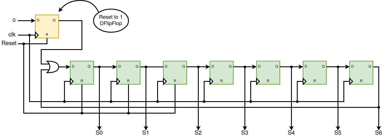
    entity SevenState_sm is
    Port(
        clk : in STD_LOGIC;
        reset : in STD_LOGIC;

        S0, S1, S2, S3, S4, S5, S6 : out STD_LOGIC
    );
    end SevenState_sm;

    architecture Behavioral of SevenState_sm is

    -- Components code here

    signal
    DFFS_D, DFFS_Q,
    DFF0_D, DFF0_Q,
    DFF1_D, DFF1_Q,
    DFF2_D, DFF2_Q,
    DFF3_D, DFF3_Q,
    DFF4_D, DFF4_Q,
    DFF5_D, DFF5_Q,
    DFF6_D, DFF6_Q : STD_LOGIC;

    begin
    DFFS_D <= '0';
    DFF0_D <= DFF6_Q or DFFS_Q;
    DFF1_D <= DFF0_Q;
    DFF2_D <= DFF1_Q;
    DFF3_D <= DFF2_Q;
    DFF4_D <= DFF3_Q;
    DFF5_D <= DFF4_Q;
    DFF6_D <= DFF5_Q;

    DFFS: DFlipFlopRA port map (DFFS_D, clk, reset, DFFS_Q);
    DFF0: DFlipFlop port map (DFF0_D, clk, reset, DFF0_Q);
    DFF1: DFlipFlop port map (DFF1_D, clk, reset, DFF1_Q);
    DFF2: DFlipFlop port map (DFF2_D, clk, reset, DFF2_Q);
    DFF3: DFlipFlop port map (DFF3_D, clk, reset, DFF3_Q);
    DFF4: DFlipFlop port map (DFF4_D, clk, reset, DFF4_Q);
    DFF5: DFlipFlop port map (DFF5_D, clk, reset, DFF5_Q);
    DFF6: DFlipFlop port map (DFF6_D, clk, reset, DFF6_Q);

    S0 <= DFF0_Q;
    S1 <= DFF1_Q;
    S2 <= DFF2_Q;
    S3 <= DFF3_Q;
    S4 <= DFF4_Q;
    S5 <= DFF5_Q;
    S6 <= DFF6_Q;
    end Behavioral;
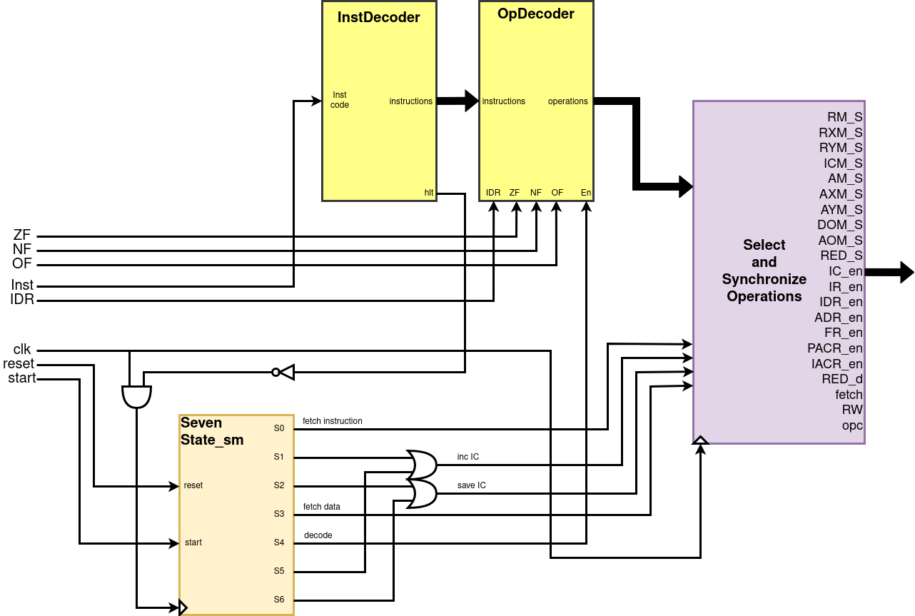
With the state machine built, we can now build our control unit to operate based on the output of the state machine's state. Fig.13 shows the control unit we'll build. As you can see it is composed of four main components:
- The state machine we just built to differentiate each instruction step.
- The instruction decoder which is just a demultiplexer using the opcode as the input selector and outputting a bit per instruction (the bit corresponding to the decoded instruction is set to 1 and the rest to 0).
- The operation decoder which receives as input the decoded instruction and relevant flags, and outputs the operations that need to be preformed on the CPU like enabling a register, selecting a specific input from a multiplexer, selecting a specific output from a demultiplexer, enable writes to the RAM module, or selecting a operation to perform on the ALU.
- Finally, the select and synchronize operations isn't actually a component, but rather a logical aggregation of operations that are performed directly in the control unit module. This "module" triggers the necessary operations for all the instruction steps that aren't the decode and execute step. When the state machine is in the decode and execute step, the operations outputted by the operation decoder are triggered. Also, all the register enable operations are ANDed to the clock signal, as described in chapter 4, to ensure the state of the registers is only updated during clock pulses.
As already stated, the instruction decoder is just a glorified demultiplexer so we'll skip its VHDL implementation. We'll now go through the
implementation of the operation decoder. The module has as output, all the possible operations that can be performed on the various components
of the CPU, this is, all of the inputs of these components. We therefore need to first figure out, which operations (or component inputs) we
want to trigger in each CPU instruction. Lets start with the first instruction: add RX RY. In order to perform this instruction
we need to set the ALU's first operand to RX and the second operand to RY, set the ALU's opcode to the add operation and finally,
enable the accumulator register (PACR). We can achieve this by triggering the following operations:
- Set the ALU's operand A selector to
0b0(so that the routed input is RX). - Set the ALU's operand B selector to
0b0(so that the routed input is RY). - Set the ALU's opcode to
0b000(add opcode). - Set the PACR enable to 1 (save the result of the addition).
After knowing all the relationships between each instruction, and the low-level operations that need to be triggered to preform the instruction, we can
implement the operation decoder module by defining each operation/output as the OR between all the instructions that require that operation/output to be set to 1.
Note that some instructions also take into account flags to trigger (or not) certain operations, like for example the instruction jmpz, which
is only performed if the zero flag is set.
To make our lives easier, I developed a small python script that takes as input the list we saw previously, and outputs the body of the corresponding module.
Although this script handles most of the modules body, we still have to take into account some important details that will be programmed manually.
Namely, many of our instructions operate over general purpose registers RX and RY. The indices X and Y are both passed in the instruction data.
Index X is stored in the first 4 bits (or 8 bits in case of a 16 bit architecture) of the instruction data and index Y in the last 4 bits (or 8 bits).
The 8 registers are aggregated into a single block like we can see in Fig.12. We use a demultiplexer when we want to update the state of a specific register,
and two multiplexer to route the value of specific registers to the rest of the CPU. The first operation (update the state of a register) is always performed
on index X (since load instructions are always performed over RX). This means that the selector of the multiplexer is simply directly wired to the first 4 bits of
the IDR (Instruction Data Register).
For the second operation (routing the output of a register to the rest of the CPU) we need to consider routing both the RX and RY registers to deal
with instructions that operate over two operands, like add RX RY. This means that the selector of the multiplexer on the left is wired to the
first 4 bits of the IDR, and the multiplexer on the right is wired to the last 4 bits of the IDR.
Finally, also note that the flag register enable can be wired to the same signal as the PACR register enable, given that whenever we store the the ALU's result in the PACR register we also of course want to update the flag register.
The final VHDL module code for this operation decoder is the following:
    entity OpDecoder is
    Port(

        En : in STD_LOGIC;
        ZF, NF, OVF : in STD_LOGIC;
        IDR_l, IDR_h : STD_LOGIC_VECTOR(7 downto 0);

        add_RX_RY,
        sub_RX_RY,
        ssp_V,
        inc_RX,
        dec_RX,
        neg_RX,
        not_RX,
        and_RX_RY,
        or_RX_RY,
        lod_V_ADR,
        str_V_mADR,
        lod_mADR_RX,
        str_RX_mADR,
        lod_RX_ADR,
        lod_ACR_RX,
        lod_ACR_ADR,
        str_ACR_mADR,
        str_IC_mADR,
        jmp_ADR,
        jmp_X,
        jmpz_X,
        jmpn_X,
        jmpo_X,
        hlt : in STD_LOGIC;

        opc : OUT STD_LOGIC_VECTOR(2 downto 0);
        RM_S : OUT STD_LOGIC;
        RXM_S : OUT STD_LOGIC_VECTOR(2 downto 0);
        RYM_S : OUT STD_LOGIC_VECTOR(2 downto 0);
        ICM_S : OUT STD_LOGIC_VECTOR(1 downto 0);
        AM_S : OUT STD_LOGIC_VECTOR(1 downto 0);
        AXM_S : OUT STD_LOGIC;
        AYM_S : OUT STD_LOGIC;
        DOM_S : OUT STD_LOGIC_VECTOR(1 downto 0);
        AOM_S : OUT STD_LOGIC;
        RED_S : OUT STD_LOGIC_VECTOR(2 downto 0);
        IC_En,
        IR_En,
        IDR_En,
        ADR_En,
        ACR_En,
        GPR_En : OUT STD_LOGIC;
        rw : OUT STD_LOGIC
    );
    end OpDecoder;

    architecture Behavioral of OpDecoder is
    -- Components code here
    signal RXM_S_8b : STD_LOGIC_VECTOR(7 downto 0);
    begin

        ACR_En <= En and (add_RX_RY or sub_RX_RY or ssp_V or inc_RX or dec_RX or neg_RX or not_RX or and_RX_RY or or_RX_RY);
        opc(0) <= En and (sub_RX_RY or ssp_V or dec_RX or not_RX or or_RX_RY);
        AYM_S <= En and (ssp_V);
        opc(1) <= En and (inc_RX or dec_RX or and_RX_RY or or_RX_RY);
        opc(2) <= En and (neg_RX or not_RX or and_RX_RY or or_RX_RY);
        AM_S(1) <= En and (lod_V_ADR);
        ADR_En <= En and (lod_V_ADR or lod_RX_ADR or lod_ACR_ADR);
        DOM_S(0) <= En and (str_V_mADR or str_IC_mADR);
        DOM_S(1) <= En and (str_V_mADR or str_ACR_mADR);
        AOM_S <= En and (str_V_mADR or lod_mADR_RX or str_RX_mADR or str_ACR_mADR or str_IC_mADR);
        rw <= En and (str_V_mADR or str_RX_mADR or str_ACR_mADR or str_IC_mADR);
        RM_S <= En and (lod_mADR_RX);
        GPR_En <= En and (lod_mADR_RX or lod_ACR_RX);
        AM_S(0) <= En and (lod_ACR_ADR);
        ICM_S(1) <= En and (jmp_ADR);
        IC_En <= En and (jmp_ADR or jmp_X or (jmpz_X and ZF) or (jmpn_X and NF) or (jmpo_X and OVF));
        ICM_S(0) <= En and (jmp_X or (jmpz_X and ZF) or (jmpn_X and NF) or (jmpo_X and OVF));

        RXM_S <= RXM_S_8b(2 downto 0);
        RYM_S <= IDR_h(2 downto 0);
        RED_S <= IDR_l(2 downto 0);


        RX_MUX: Mux2_8b port map (
            I0 => IDR_l,
            I1 => "00000111",
            sel => ssp_V,
            o => RXM_S_8b
        );

        AXM_S <= '0';
        IDR_En <= '0';
        IR_En <= '0';
    end Behavioral;
As we discussed previously, the select and synchronize operations "module" is just a logical aggregation of operations that are performed directly in the control unit module. Given that some of the instruction steps, like Increment IC and Load Increment, also need to trigger operations like the instructions during the Decode and Execute step, a bunch of OR and AND gates are used to select the necessary operations depending on the current state of the state-machine and the operations selected by the operation decoder. All the enable operations are also ANDed to the clock signal as already stated.

One important detail is that the register enable operations are actually ANDed to the inverted clock signal (clock signal followed by a NOT gate) instead of the raw clock signal. This results in the registers being updated on the down pulses (clock change from 1 to 0). Fig.15 shows why this is important. The state-machine state changes are triggered during the up clock pulses (clock change from 0 to 1), meaning that the instruction decoding and/or operation selection, for a given instruction, starts right after such a pulse. If we were to update the registers during the up clock pulses as well, we would get signal propagation delay related glitches. We would update the registers before the correct input data would reach the registers. To ensure this doesn't happen, the registers are updated on the down clock pulses, right at the middle point of a clock cycle.
The VHDL code for the control unit is quite long, so I won't include it in this document, but it can be found here.
Finally, with the control unit built, the full CPU module can easily be implemented by wiring all the components we have just built as seen in Fig.12. Since the code for the module is quite extensive and not particularly interesting, I also won't include it in this document, but it can be found here, and this is what the entity's port looks like:
    entity CPU is
    Port(
        reset : in STD_LOGIC;
        clk : in STD_LOGIC;
        dataIn : in STD_LOGIC_VECTOR(7 downto 0);

        address : out STD_LOGIC_VECTOR(7 downto 0);
        dataOut : out STD_LOGIC_VECTOR(7 downto 0);
        readWrite : out STD_LOGIC;
        fetch : out STD_LOGIC;
    );
    end CPU;
Similarly, the main module also just involves wiring the CPU module with the memory modules. To switch between the RAM and ROM modules, a the fetch signal (controlled by the control unit) is used to enable and disable the two memory modules. Whenever fetch is set to 1, to ROM module is enabled and the RAM disabled, and vice-versa. The fetch signal is only set to zero during the Decode and Execute step.
7. Executing a Program
With the CPU built, its time to write and execute our first program. Given that our program will reside in the ROM, at this point, writing and loading a program into our CPU, is achieved by manually writing the instructions in binary in the correct address lines. To start simple, we'll write a program that multiplies two numbers (given that our ALU doesn't directly support multiplication). In C we could easily implement a multiplication program using only addition and looping as follows:
    int a = 3;
    int b = 5;
    int res = 0;

    for(int i = 0; i < b; i++) {

        res += a;
    }
In our CPU, we can assume that register RA, RB, RC and RD hold the variables a, b, res and i respectively. The loop can then be implemented using a set of additions and some conditional jumps. Here is the assembly code that expresses the previous program:
    ; a = 3
    lod $3 RA

    ; b = 5
    lod $5 RB

    ; res = 0
    lod $0 RC

    ; i = 0
    lod $0 RD

    loop_start:

        ; res += a
        add RC RA
        lod ACR RC

        ; i++
        inc RD
        lod ACR RD

        ; if i < b goto loop_start
        sub RD RB
        jmpn loop_start

    hlt
Note that loading a specific value to a specific register (lod $V RX) is actually achieved using two instructions instead of the single
instruction like we used in the previous code. This operation can be performed as follows
(assuming ADR is set to an unused address like 0x3e):
    str $V [ADR]
    lod [ADR] RX
Finally we have to translate this assembly, into machine code:
| address | instruction | opcode | data | description |
|---|---|---|---|---|
| 0b00000000 | lod $0x3e ADR | 0b00001001 | setup ADR | |
| 0b00000001 | 0b00111110 | |||
| 0b00000010 | str $3 [ADR] | 0b00001010 | a = 3 | |
| 0b00000011 | 0b00000011 | |||
| 0b00000100 | lod [ADR] RA | 0b00001011 | ||
| 0b00000101 | 0b00000000 | |||
| 0b00000110 | str $5 [ADR] | 0b00001010 | b = 5 | |
| 0b00000111 | 0b00000101 | |||
| 0b00001000 | lod [ADR] RB | 0b00001011 | ||
| 0b00001001 | 0b00000001 | |||
| 0b00001010 | str $0 [ADR] | 0b00001010 | res = 0 | |
| 0b00001011 | 0b00000000 | |||
| 0b00001100 | lod [ADR] RC | 0b00001011 | ||
| 0b00001101 | 0b00000010 | |||
| 0b00001110 | str $0 [ADR] | 0b00001010 | i = 0 | |
| 0b00001111 | 0b00000000 | |||
| 0b00010000 | lod [ADR] RD | 0b00001011 | ||
| 0b00010001 | 0b00000011 | |||
| 0b00010010 | add RC RA | 0b00000000 | res += a | |
| 0b00010011 | 0b00000010 | |||
| 0b00010100 | lod ACR RC | 0b00001110 | ||
| 0b00010101 | 0b00000010 | |||
| 0b00010110 | inc RD | 0b00000011 | i++ | |
| 0b00010111 | 0b00000011 | |||
| 0b00011000 | lod ACR RD | 0b00001110 | ||
| 0b00011001 | 0b00000011 | |||
| 0b00011010 | sub RD RB | 0b00000001 | if i < b goto loop_start | |
| 0b00011011 | 0b00010011 | |||
| 0b00011100 | jmpn loop_start | 0b00010101 | ||
| 0b00011101 | 0b00010010 | |||
| 0b00011110 | hlt | 0b00010111 | halt | |
| 0b00011111 | 0b00000000 |
We now use this machine-code to update our ROM module with the instructions and instruction-data in the corresponding addresses:
    entity ROM is
    Port(
        adr : in STD_LOGIC_VECTOR(7 downto 0);
        En : in STD_LOGIC;
        DO : out STD_LOGIC_VECTOR(7 downto 0)
    );
    end ROM;

    architecture Behavioral of ROM is
    begin
    process(adr, En)
    begin
        if En = '0' then
            DO <= "00000000";
        else

            case adr is
                when "00000000" => DO <= "00001001";
                when "00000001" => DO <= "00111110";
                when "00000010" => DO <= "00001010";
                when "00000011" => DO <= "00000011";
                when "00000100" => DO <= "00001011";
                when "00000101" => DO <= "00000000";
                when "00000110" => DO <= "00001001";
                when "00000111" => DO <= "00111110";
                when "00001000" => DO <= "00001010";
                when "00001001" => DO <= "00000101";
                when "00001010" => DO <= "00001011";
                when "00001011" => DO <= "00000001";
                when "00001100" => DO <= "00001001";
                when "00001101" => DO <= "00111110";
                when "00001110" => DO <= "00001010";
                when "00001111" => DO <= "00000000";

                -- ...

                when others => DO <= "00000000";
            end case;
        end if;
    end process;
    end Behavioral;
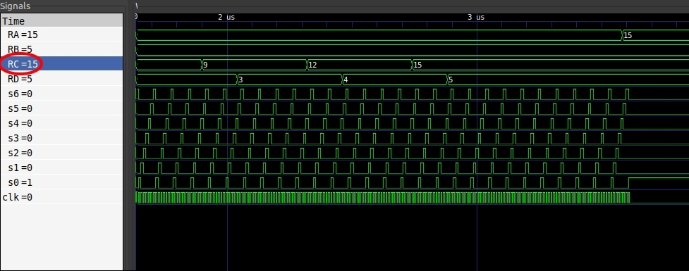
Finally, we can write a simple VHDL test for our Main module, simulate it using ghdl, and view the simulation using GTKWave. As you can see in Fig.16 the final result stored in register RC (representing our variable res) is 15! The result of 3*5.
8. Assembler
As you may have noticed, translating assembly into machine code is quite time consuming and tedious. This is where an assembler comes in handy. I've implemented a simpler assembler for our ISA in python. I won't give a detailed guide on how to implement such an assembler given that this could become a whole new guide on its own. Another reason, is that the assembler I've implemented is of relatively low quality as it doesn't really follow the usual structure of a compiler/assembler (lexer, parser, code generator, etc), but rather, it just uses a bunch of string manipulations to get the job done. I also included a ROM generator which turns the outputed machine code from the assembler into a VHDL ROM module which we can load into our VHDL project.
To make our lives easier, we can also add a set of macros to the assembler to avoid rewriting repetitive code patterns. A macro,
is a "fake" instruction, which is expanded into a set o multiple instructions of our ISA during assembly. For example, in chapter 7
we saw it would be useful to have a lod $V RX instruction, which can be achieved by executing two existing instructions.
Our assembler includes the following macros:
    lod $V RX (load value to register):
        lod $62 ADR
        str $V [ADR]
        lod [ADR] RX

    psh ($V or RX) (push value or register to the top of the stack):
        lod SP ADR
        str ($V or RX) [ADR]
        inc SP
        lod ACR SP

    pop RX (pop top of stack to RX):
        dec SP
        lod ACR SP
        lod SP ADR
        lod [ADR] RX

    pop (pop top of stack):
        dec SP
        lod ACR SP

    lsr $V RX (Load Stack variable V to Register RX):
        sub SP $V
        lod ACR ADR
        lod [ADR] RX

    srs RX $V (Store Register RX to Stack variable V):
        sub SP $V
        lod ACR ADR
        str RX [ADR]
Another quality of life improvement offered by the assembler, is allowing the programmer to use labels instead of addresses for jump instructions. During
assembly the labels are converted to the corresponding memory address.
With all these features, we can more easily test more complex programs. In the following program
we define an average function, which given an array and its length, calculates its average (note: ; initiates a line comment):
    ; list average program
    ; avg( [5,2,9] ) = 5

    jmp main

    avg:

        ; arr
        pop RB
        ; len
        pop RC
        ; sum = 0
        lod $0 RD
        ; i = 0
        lod $0 RE

        sum_loop_start:

            ; if i >= len goto loop_end
            sub RC RE
            jmpn sum_loop_end
            jmpz sum_loop_end

            ; sum += arr[i]
            add RB RE
            lod ACR ADR
            lod [ADR] RF
            add RD RF
            lod ACR RD

            ; i++
            inc RE
            lod ACR RE
            jmp sum_loop_start


        sum_loop_end:

        ; div = 0
        psh $0
        ; s = sum
        psh RD

        div_loop_start:

            ; s -= len
            lsr $1 RF
            sub RF RC
            lod ACR RF
            srs RF $1

            ; if s <= 0 goto div_loop_end
            lsr $1 RF
            dec RF
            jmpn div_loop_end

            ; else div++ and goto div_loop_start
            lsr $2 RF
            inc RF
            lod ACR RF
            srs RF $2
            jmp div_loop_start

        div_loop_end:

        ; return div
        pop
        pop RA
        pop RB
        lod RB ADR
        jmp ADR

    main:

        ; len = 3
        psh $3
        ; arr[0] = 5
        psh $5
        ; arr[1] = 2
        psh $2
        ; arr[2] = 9
        psh $9


        ; psh return line
        psh avg_ret
        ; psh len
        lsr $5 RA
        psh RA
        ; psh arr
        SSP $5
        psh ACR
        ; call avg(arr,len)
        jmp avg
        avg_ret:

        hlt
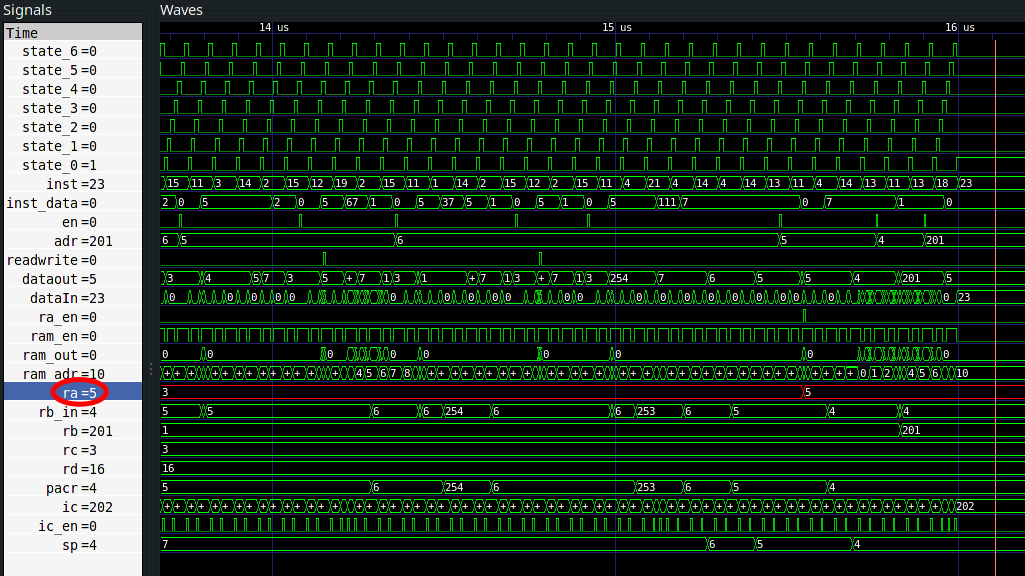
After assembling the program into machine code and generating the ROM module, we can simulate the CPU once again in ghdl, and view
the result of the simulation using GTKWave. As seen in Fig.17, the result stored in register RA is 5 which is indeed
the average of the input array arr = [5, 2, 9].
9. FPGA
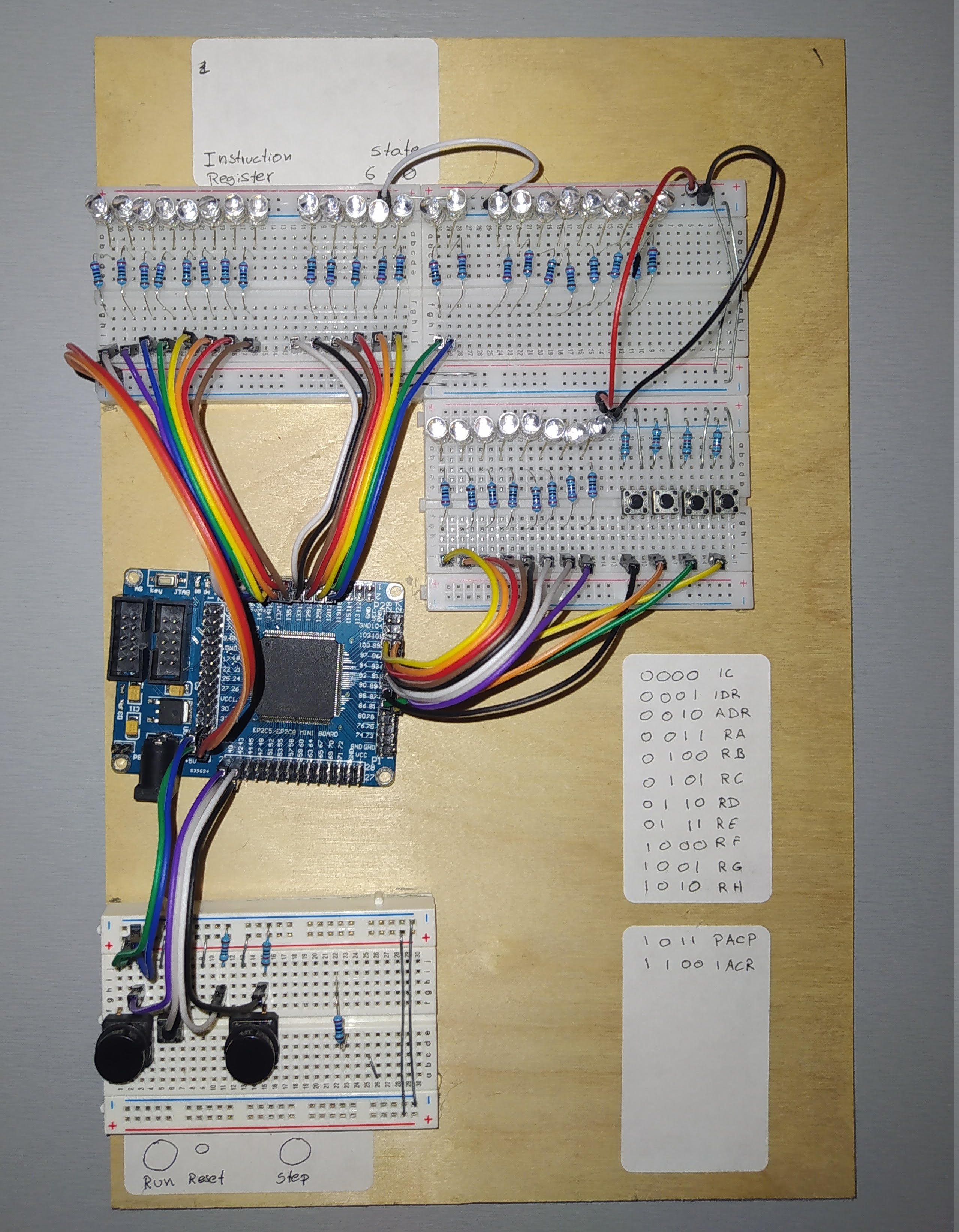
Once I was able to implement and execute "complex" programs on the DCPU, I decided to buy a cheap FPGA (the ALTERA CycloneII EP2C5T144) and load it on real Hardware as seen in Fig.18. This required some additional coding and configuration, namely:
- Adding more outputs to some of the modules to have them accessible to the GPIO pins of the board.
- Adding modules to switch between various outputed registers.
- Adding modules to deal with contact debounce on switches.
- Configuring the board using Intel Quartus II Web Edition.
This step is of course not very crucial for this project, but is quite fun since you are able to view and interact with the CPU in real time. It also allows us to later connect our CPU to other hardware and start thinking about IO. If you are interested in this particular board, I recommend the following this video which gives a great introduction on the process of configuring it using Quartus II.